Samsung Foundry Broadcom Deal: The 2nm Chips Aren’t AI Chips
- The sub-2nm volume Samsung takes from Broadcom is not AI accelerator silicon. Samsung’s own press release scopes it to “Broadcom products including WBC (Wireless Broadband Communications) solutions,” and Reuters described it as Broadcom’s “next-generation communications chips.”
- So I read the Samsung foundry Broadcom deal not as taking AI silicon away from TSMC, but as the first live test of selling memory, logic and advanced packaging as one bundle — aimed squarely at the packaging bottleneck TSMC’s own CEO admitted to on the July 16 call.
- I have not bought. It is a non-binding MOU, and this foundry has watched the same story play out three times already with Qualcomm, Google and Tesla.
All weekend the headline collapsed into one sentence: Samsung won $200 billion from Broadcom and is finally closing on TSMC. On Saturday morning I read it that way too.
Then, while writing the piece mapping the whole summit across four axes, I started opening the primary documents behind each deal one at a time. I opened Samsung’s own English newsroom release dated July 25 and my reading changed. Everyone is looking at the $200 billion figure and at foundry market share. The actual news was sitting in the object of the sentence.
Contents
What the Samsung foundry Broadcom deal actually scopes to 2nm
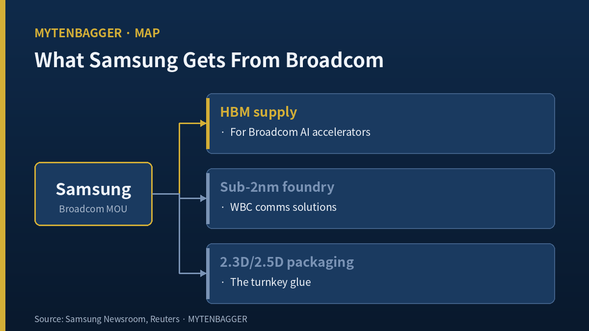
Samsung’s July 25 release splits the cooperation into three strands. First, HBM supply for Broadcom’s next-generation AI accelerators. Second, manufacturing of Broadcom products including WBC (Wireless Broadband Communications) solutions on sub-2nm process technology. Third, 2.3D and 2.5D advanced packaging.
The strands are separate sentences. “AI accelerator” attaches to the memory line. The object attached to sub-2nm foundry is communications solutions. Reuters, in its July 24 piece by Max A. Cherney and Heekyong Yang, points the same direction: Samsung will manufacture Broadcom’s “next-generation communications chips” using sub-2-nanometre process technology.
Downstream coverage blurred the line. Fortune, picking up Bloomberg, bundled it as “AI accelerators and networking silicon.” Several outlets went further and described the foundry portion outright as AI accelerator logic. Most Korean-language coverage did the same.
Context on where this sits, for anyone arriving here first. The $200 billion is one slice of roughly $950 billion in cooperation announced at the July 24 San Francisco summit, and the largest single slice — about $500 billion between SK and Nvidia — is a letter of intent rather than a contract. Korea’s presidential policy chief characterised the semiconductor portion of the package as five-year long-term purchase commitments rather than inbound investment. So the base rate for converting these announcements into revenue is the thing to hold in mind before pricing any of them.
The two highest-confidence sources — Samsung’s own release and Reuters — both point at communications. I have not yet found a named reporter or analyst who makes this distinction explicitly.
I will admit this deflated me a little. I had Samsung’s English and Korean releases open side by side and spent longer than I want to say staring at the acronym WBC. Communications silicon and AI accelerators differ in die size, in volume structure, in revenue per wafer. More importantly, the “took AI volume from TSMC” story does not survive it. Broadcom’s AI XPU work still runs through TSMC. Whether this volume is transferred from TSMC or incremental on top of it has not been stated by either company.
But stopping there is reading half of it. Once I had the object right, the actual content of the deal got sharper. What Samsung sold is not one process node. It is HBM and logic and 2.3D/2.5D packaging as a single bundle. Jun Young-hyun, who heads Samsung’s Device Solutions division, is quoted in the same release saying that in the AI era what matters is semiconductor solutions where memory, logic and advanced packaging are tightly integrated. Read against the scope, that is not marketing language. It is the blueprint.
Three reasons I keep watching the Samsung foundry Broadcom deal anyway
One — TSMC’s CEO named the bottleneck himself
TSMC’s second quarter of 2026 was overwhelming. Revenue of $40.20 billion, up 36.0% year on year. Gross margin 67.7%. Net income up 77.4%. It also raised 2026 capital expenditure guidance from $52–56 billion to $60–64 billion.
And on the July 16 call, the CEO of that company said this: “our packaging capacity is so tight that now it’s limiting my customers’ growth.” That is C.C. Wei’s own phrasing. TrendForce puts TSMC’s CoWoS target at roughly 120,000–140,000 wafers per month in 2026, with the supply gap narrowing from about 20% to 10% — narrowing, but still a gap.
This is why I read the deal as a bypass around a packaging constraint rather than a fight over foundry share. From Broadcom’s seat, Samsung is not a replacement for TSMC. It is a second window that can absorb what TSMC cannot take, with memory attached.
Two — the buyer is Broadcom, and that matters on its own
Broadcom’s fiscal Q2 2026, reported June 3, showed total revenue of $22.19 billion, up 48% year on year, of which AI semiconductor revenue was $10.8 billion, up 143%. Third-quarter guidance calls for $16.0 billion in AI semiconductors alone.
CEO Hock Tan’s numbers on that call ran larger still: $56 billion of AI semiconductor revenue for fiscal 2026 and “in excess of $100 billion” for fiscal 2027. The XPU customers he named on the record were Google, Anthropic, OpenAI and Meta.
Concentrating that volume in a single foundry is a procurement risk. Broadcom diversifying capacity is not affection for Samsung; it is arithmetic driven by volume it genuinely has. That the motive is arithmetic rather than sentiment is the reason I cannot dismiss this deal outright.
Three — the memory half is already proven
The foundry half is a promise. The memory half is not. Samsung stated in a March 17 release that HBM4 was in mass production, and on May 29 shipped the industry’s first HBM4E 12-high samples. On June 5, Nvidia certified Samsung, SK hynix and Micron for Vera Rubin. Nvidia has not disclosed how the volume splits among them.
Samsung’s preliminary second-quarter numbers were revenue of ₩171 trillion (about $118 billion) and operating profit of ₩89.4 trillion (about $61 billion), converted at roughly ₩1,455 to the dollar — my own arithmetic. Operating profit was up 1,810% year on year. I counted the digits twice the first time I saw it.
The memory position underneath that is more contested than the headline suggests, and I want to put both sides of it down. In commodity DRAM, Samsung retook first place in Q1 2026 at 38.5% share on TrendForce’s count, ahead of SK hynix. In HBM specifically it is a different picture: Counterpoint has SK hynix at 58% for the same quarter, with Samsung and Micron level at roughly 21% each.
Those two facts together are the actual state of play. Samsung is the volume leader in memory broadly and the number-three-tied player in the part of memory that AI accelerators consume. The June 5 three-way Vera Rubin certification is what makes this interesting — it means Samsung is qualified rather than winning, and the gap between qualified and winning is entirely an allocation decision that Nvidia has not published.
For a US reader the cleanest way to hold this is that Micron, listed and priced at home, sits on the same 21% rung as Samsung in HBM. If you believe HBM4 volumes broadly, that is a position you can take without touching the Korea Exchange at all. What you cannot get from Micron is the bundle — and the bundle is the entire subject of this piece.
The numbers around the Samsung foundry Broadcom deal
| Q1 2026 foundry | Share | Revenue |
|---|---|---|
| TSMC | 72% | $35.86bn |
| Samsung | 6.5% | $3.2bn |
| Revenue gap | — | roughly 11x (my calculation) |
Source: TrendForce, Q1 2026. Another tally puts TSMC at 67.6%, so I do not treat this as a single settled figure.
Spread the $200 billion across five years and it is $40 billion a year — again my own division, and no source frames it that way. More to the point, the split between memory, foundry and packaging has not been disclosed anywhere. Modeling a share recovery without knowing the foundry slice is not analysis.
For the forward view I use only named reports, all published before the summit. KB Securities analyst Kim Dong-won raised his objective to ₩600,000 on July 8. Shinhan Investment’s Kim Hyung-tae went to ₩590,000 on June 30. Meritz Securities’ Kim Sun-woo moved to ₩500,000 on July 6. Goldman Sachs’ Giuni Lee published ₩480,000 on July 8, arguing a forward P/E of 5.3x against a long-run average near 14x. Kiwoom Securities’ Park Yu-ak was the only one to cut, to ₩390,000 on July 8.
That is a spread of roughly 54% between the high and the low, on reports published within nine days of each other. One clarification, because it gets misquoted: Kiwoom’s cut rests on a slowing second-half EPS growth rate, not on valuation. Those are different arguments and conflating them misreads the note. These are third-party figures I am citing, not numbers I have adopted.
A practical note for readers outside Korea. Samsung Electronics trades on the KOSPI, Korea’s main board — the KOSDAQ is the smaller-cap venue — and there is no ordinary US-listed ADR line for it. If you want the Broadcom side of this trade instead, that one is listed at home and priced daily.
Why the Samsung foundry Broadcom deal is a bundle, and when a bundle stops working
It is worth being concrete about what “turnkey” means here, because it is the part US readers have the least visibility into and it is the only structural argument in Samsung’s favour that does not depend on catching TSMC.
Building a Broadcom XPU today means three separate procurements. The logic die is fabricated at a foundry. The HBM stacks are bought from a memory maker — SK hynix, Samsung or Micron. Then the two are married in advanced packaging, which for leading-edge parts overwhelmingly means TSMC’s CoWoS. Three vendors, three queues, three sets of qualification.
Samsung is the only company on earth that can quote all three from inside one corporate boundary. TSMC has world-leading logic and packaging and no memory at all. SK hynix leads in HBM and has no foundry. Intel has logic and packaging but no leading-edge HBM of its own. Look again at the three strands in the July 25 release — HBM, sub-2nm logic, 2.3D/2.5D packaging — and you are looking at the only combination that could have been written by any single company.
Now the part that keeps me honest about it. Being able to do all three is not the same as being best at any of them. Samsung holds 6.5% of foundry against TSMC’s 72%, and roughly 21% of the HBM market against SK hynix’s 58% in Q1 2026 per Counterpoint. A bundle assembled from second-place parts is only attractive while the first-place parts are rationed.
Which is exactly the condition C.C. Wei described on July 16 — and conditions expire. TrendForce already has the CoWoS supply gap narrowing from around 20% to 10%. If TSMC’s packaging capacity catches up with demand in 2027, the scarcity that makes the bundle worth buying goes away, and Broadcom has no particular reason to keep a second window open. So the turnkey thesis is not a moat. It is a lease on a shortage. That is a materially different thing to own, and it is why I treat this as something to watch rather than something to size.
The pattern this foundry has repeated three times
Here is the real reason I am not excited. Large announcements failing to arrive as revenue is not a one-off here.
Qualcomm switched three times. It put Snapdragon 8 Gen 1 on Samsung 4nm in 2022, then moved follow-on volume to TSMC over thermal and yield issues. In March 2025 it skipped Samsung entirely for Snapdragon 8s Gen 4, choosing TSMC 4nm. In April 2026 reporting emerged that its next flagship was under review for a full move to TSMC N2P.
Google left outright. Tensor moved to TSMC from the G5 generation, with reporting indicating the following generation is committed as well.
Tesla slipped and split. AI6 is a real contract — $16.5 billion, disclosed to Korea’s regulatory filing system in July 2025, running to the end of 2033. Yet prototype timing slipped roughly six months, pushing volume production toward late 2027 per Electrek’s reporting, and follow-on silicon was reported as allocated to TSMC’s Arizona site. Even the win most often cited as Samsung foundry’s biggest looks like this up close.
And this one is a non-binding MOU. As TipRanks noted on July 25, the document sets out intent without annual purchase targets or a spending start date. Reuters wrote “up to $200 billion” — a ceiling, not a floor.
On the cycle side, Bloomberg Intelligence’s Shuli Ren has argued the global memory shortage likely peaked in the second quarter of 2026, pointing to simultaneous expansion at Samsung, SK hynix and Micron and raising the possibility of oversupply by 2028. The bulls are still the majority. Being the majority is not the same as being right.
Three paths for the Samsung foundry Broadcom deal
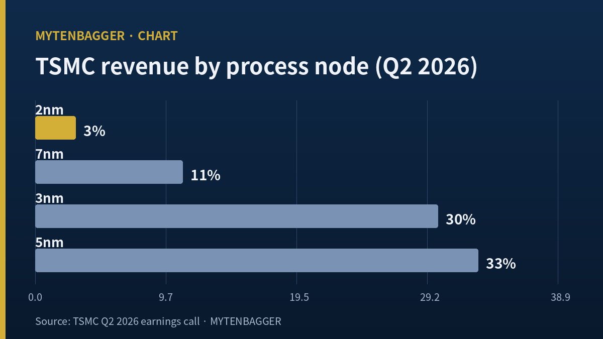
One more number belongs here. TSMC disclosed its Q2 2026 revenue by node: 5nm 33%, 3nm 30%, 7nm 11% — and 2nm at 3%, with advanced nodes at 7nm and below making up 77% of the total.
That figure reset my sense of timing. 2nm is at the very start of its revenue curve. This is not Samsung chasing a mature node from behind; it is closer to getting another at-bat in the first inning. Which cuts both ways — an early inning means plenty of time for TSMC too. Not an advantage, just not over.
My base case, roughly 55%. Communications silicon and HBM genuinely run, packaged volume starts landing as revenue around 2027, and the AI accelerator core stays at TSMC. Foundry share does not move meaningfully; the earnings improvement comes from memory and packaging. This is the scenario where the disclosed language runs exactly as written.
Where I am wrong, roughly 25%. Broadcom moves some XPU volume to Samsung. If more than $100 billion of fiscal 2027 AI semiconductor revenue cannot be absorbed by TSMC capacity alone, that branch is entirely plausible. In that case my reading above is half wrong and I recalculate.
The bad path, roughly 20%. The non-binding MOU never converts into specific orders and quietly fades. That is the Qualcomm and Google ending, and the $200 billion stays a number. I hold it at 20% rather than higher for exactly one reason: this buyer is genuinely capacity-constrained.
What would break my read on the Samsung foundry Broadcom deal
My checkpoints are not equally weighted, so I list them by weight.
Heaviest by far — does the scope move past communications silicon? If it is officially confirmed that Broadcom volume at Samsung extends beyond WBC into XPU or accelerator families, the character of this deal changes and my “turnkey first test” reading has to be rebuilt along with the caution attached to it. This single item outweighs the other two combined.
Next — Taylor fab 2nm production start and the Tesla schedule. If that slips again, I will not trust the first checkpoint even if it reads well. Where execution has repeatedly slid, the evidence is a running line, not a signed contract.
Lightest, but continuous — foundry segment profitability. Samsung does not break out foundry P&L, so I am left reading the qualitative commentary on the earnings call: whether the phrase “narrowing losses” appears, and what conditions get attached when it does.
If the first does not move, the second and third can both come in well and this stays a communications deal. If the first does move, I will lower my bar on the other two and rerun the numbers. That is how differently they weigh.
So what am I doing
Nothing. I did not buy. As I wrote in the summit opener, I am poor at buying names that fall on record earnings days, and Samsung fell more than 6% on July 7 when preliminary Q2 results landed, then fell hard again after. Freezing at that kind of price is a weakness of mine, not a discipline, so I record it as such.
What I did do this weekend is specific. I opened the primary release instead of the headline, and one grammatical object made me rewrite my whole reading of the deal. I started at “took it from TSMC.” I ended at “walked into the gap where TSMC is packaging-constrained, carrying memory.” The second is less thrilling and I think it is the bigger of the two. Selling a bundle tends to outlast selling a node.
The next piece in this series takes the power and network infrastructure axis, breaking the summit’s 5GW down by where it physically jams. Whether this read holds will be answered by whether Broadcom’s orders travel past communications silicon. Until then I am watching. That is my read of it, and I hold it loosely.
The primary material behind this: Samsung’s own release on the collaboration, TSMC’s Q2 2026 results, Broadcom’s fiscal Q2 2026 results, TrendForce on the TSMC capex raise, Electrek on the Tesla AI6 delay, and Fortune’s write-up of the arrangement. The Korean sell-side figures above come from Korean-language reports and are cited by firm, analyst and date; those are my renderings, not English-language originals.
Related reading